
Wafer Oxidation
Wafer Oxidation – Photoresist Spray System – Cheersonic
The role of the oxidation process is to form a protective film on the wafer surface. It protects wafers from chemical impurities, prevents leakage currents from entering circuits, prevents diffusion during ion implantation, and prevents wafer slippage during etching. The first step of the oxidation process is to remove impurities and pollutants, and it is necessary to remove impurities such as organics, metals, and evaporation residual moisture through four steps. Once cleaned, the wafer can be placed in a high temperature environment of 800 to 1200 degrees Celsius, where a layer of silicon dioxide (or “oxide”) is formed by the flow of oxygen or vapor over the surface of the wafer. Oxygen diffuses through the oxide layer and reacts with silicon to form an oxide layer of various thicknesses, whose thickness can be measured after the oxidation is complete.
Dry oxidation and wet oxidation According to the different oxidants in the oxidation reaction, the thermal oxidation process can be divided into dry oxidation and wet oxidation. The former uses pure oxygen to produce a silicon dioxide layer, which is slow but the oxide layer is thin and dense, and the latter The use of both oxygen and highly soluble water vapor is characterized by fast growth but relatively thick and low density protective layers.
In addition to the oxidant, there are other variables that affect the thickness of the silicon dioxide layer. First, the wafer structure and its surface defects and internal doping concentrations all affect the rate of oxide formation. In addition, the higher the pressure and temperature generated by the oxidation equipment, the faster the oxide layer will be formed. During the oxidation process, it is also necessary to use dummy wafers according to the position of the wafer in the cell to protect the wafer and reduce the difference in oxidation degree.
Ultrasonic spraying technology is used for semiconductor photoresist coating. Compared with traditional coating processes such as spin coating and dip coating, it has the advantages of high uniformity, good encapsulation of microstructures, and controllable coating area. In the past 10 years, it has been fully demonstrated that the 3D microstructure surface photoresist coating using ultrasonic spraying technology, the prepared photoresist coating is significantly higher than the traditional spin coating in terms of microstructure wrapping and uniformity Craft.
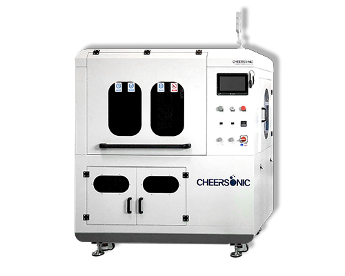
The ultrasonic spraying system can precisely control the flow rate, coating speed and deposition volume. Low-speed spray shaping defines atomized spray as a precise and controllable pattern to avoid excessive spray when producing a very thin and uniform layer. The ultrasonic spray system can control the thickness from sub-micron to more than 100 microns, and can coat any shape or size.