
Wafer Processing
Wafer Processing – Photoresist Deposition System – Cheersonic
All semiconductor processes start with a grain of sand! Because the silicon contained in the sand is the raw material needed to produce wafers. Wafers are circular slices formed by cutting a single crystal cylinder of silicon (Si) or gallium arsenide (GaAs). To extract high-purity silicon materials, silica sand, a special material with a silicon dioxide content of up to 95%, is also the main raw material for making wafers. Wafer processing is the process of producing and obtaining the above-mentioned wafers.
①Ingot casting
The sand is first heated to separate carbon monoxide and silicon, and the process is repeated until ultra-high-purity electronic-grade silicon (EG-Si) is obtained. High-purity silicon is melted into a liquid and then solidified into a single-crystal solid form called an “ingot,” the first step in semiconductor manufacturing. The manufacturing precision of silicon ingots (silicon pillars) is very high, reaching the nanometer level, and the widely used manufacturing method is the pulling method.
②Ingot cutting
After the previous step is completed, both ends of the ingot need to be cut off with a diamond saw, and then cut into thin slices of a certain thickness. The ingot flake diameter determines the wafer size, and larger and thinner wafers can be divided into more usable units, helping to reduce production costs. After cutting the silicon ingot, it is necessary to add “flat area” or “dimple” markings on the wafer, so that it is convenient to set the machining direction as a standard in subsequent steps.
③Wafer surface polishing
The thin slices obtained by the above dicing process are called “bares”, ie unprocessed “raw wafers”. The surface of the die is uneven, and it is not possible to print circuit patterns directly on it. Therefore, it is necessary to first remove surface defects through grinding and chemical etching processes, then to form a smooth surface through polishing, and then to remove residual contaminants through cleaning to obtain a finished wafer with a clean surface.
Ultrasonic spraying technology is used for semiconductor photoresist coating. Compared with traditional coating processes such as spin coating and dip coating, it has the advantages of high uniformity, good encapsulation of microstructures, and controllable coating area. In the past 10 years, it has been fully demonstrated that the 3D microstructure surface photoresist coating using ultrasonic spraying technology, the prepared photoresist coating is significantly higher than the traditional spin coating in terms of microstructure wrapping and uniformity Craft.
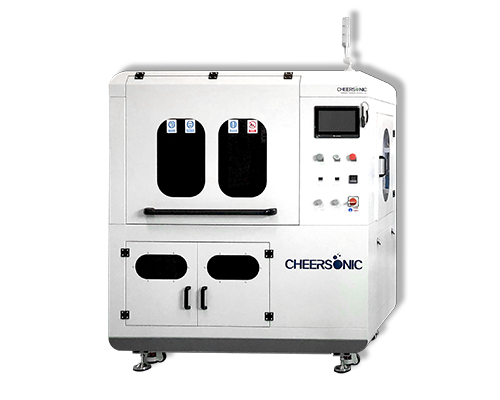
The ultrasonic spraying system can precisely control the flow rate, coating speed and deposition volume. Low-speed spray shaping defines atomized spray as a precise and controllable pattern to avoid excessive spray when producing a very thin and uniform layer. The ultrasonic spray system can control the thickness from sub-micron to more than 100 microns, and can coat any shape or size.