The Importance Of Masks
The Importance Of Masks – Semiconductor Coatings – Cheersonic
The mask is a graphic transfer tool or master in the microelectronics manufacturing process, and it is the carrier of intellectual property information such as graphic design and process technology.
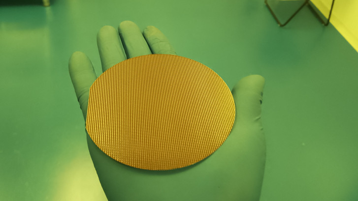
The function of the mask is similar to the “negative film” of a traditional camera. The production process is: 1. Using quartz glass as the substrate (there are other substrate materials), a layer of metal chrome and photosensitive glue is plated on it to become a photosensitive material , which is the blank mask. 2. According to the needs of downstream customers, the designed circuit pattern is exposed to the photosensitive adhesive through electronic laser equipment, the exposed area will be developed, the circuit pattern will be formed on the metal chrome, and then the unnecessary metal layer will be formed. And the adhesive layer is washed away to obtain the finished product of the mask. 3. Downstream manufacturers then use the lithography machine to print the fine circuit image on the mask on the substrate (the substrate here generally refers to a silicon wafer, but also other metal layers and dielectric layers), and then Get the chip.
It can be seen from the whole process that the mask is used for the mass production of downstream electronic components and is a key part of the production process connection in the downstream industry. The quality of the reticle will directly affect the quality of lithography, and manufacturing defects and errors on the reticle will also be introduced into chip manufacturing along with the lithography process. Therefore, the reticle is one of the determinants of the accuracy and quality of downstream products.
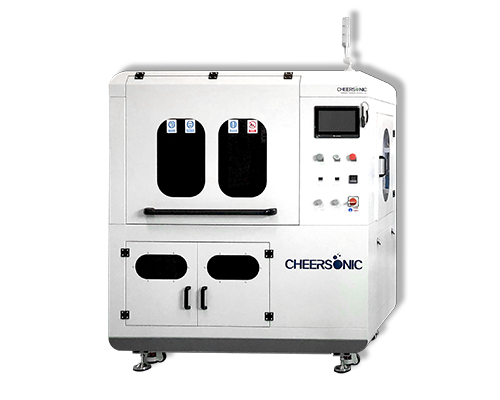
Ultrasonic spraying technology is used for semiconductor photoresist coating. Compared with traditional coating processes such as spin coating and dip coating, it has the advantages of high uniformity, good encapsulation of microstructures, and controllable coating area. In the past 10 years, it has been fully demonstrated that the 3D microstructure surface photoresist coating using ultrasonic spraying technology, the prepared photoresist coating is significantly higher than the traditional spin coating in terms of microstructure wrapping and uniformity Craft.
The ultrasonic spraying system can precisely control the flow rate, coating speed and deposition volume. Low-speed spray shaping defines atomized spray as a precise and controllable pattern to avoid excessive spray when producing a very thin and uniform layer. The ultrasonic spray system can control the thickness from sub-micron to more than 100 microns, and can coat any shape or size.