
Classification of Transistors
In the past 100 years, during the development of semiconductor transistors, pioneering scientists and engineers have constantly tried various device structures and device materials to meet the requirements of integrated circuit characteristics in different fields. Various semiconductor devices are produced.
Semiconductors are inherently abstract and elusive. The various names and abbreviations of semiconductors also make semiconductors more unpredictable, which brings many troubles to the electronics industry practitioners who are not semiconductors.
The classification of transistors can be understood from two aspects: device structure and device material.
The materials and structures of transistors are independent of each other and can be freely combined in theory. For example, BJT devices can be designed on silicon or gallium arsenide.
For the accurate description of a device, the material and device type should be described at the same time. For example, for the HBT device used in the 5G mobile phone RF PA, the exact name should be GaAs HBT device. However, due to the convention in our daily work, the name is often simplified.
For example, in the field of mobile radio frequency, we generally use HBT, or GaAs for short, GaAs HBT; In the field of power control, we use SiC for short SiC MOSFET and GaN for short GaN FET devices. This abbreviation is effective in a certain industry segment, but it may cause misunderstanding when communicating outside the industry, and should be noted when necessary.
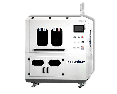
Ultrasonic spraying technology is used for semiconductor photoresist coating. Compared with traditional coating processes such as spin coating and dip coating, it has the advantages of high uniformity, good encapsulation of microstructures, and controllable coating area. In the past 10 years, it has been fully demonstrated that the 3D microstructure surface photoresist coating using ultrasonic spraying technology, the prepared photoresist coating is significantly higher than the traditional spin coating in terms of microstructure wrapping and uniformity Craft.
The ultrasonic spraying system can precisely control the flow rate, coating speed and deposition volume. Low-speed spray shaping defines atomized spray as a precise and controllable pattern to avoid excessive spray when producing a very thin and uniform layer. The ultrasonic spray system can control the thickness from sub-micron to more than 100 microns, and can coat any shape or size.
About Cheersonic
Cheersonic is the leading developer and manufacturer of ultrasonic coating systems for applying precise, thin film coatings to protect, strengthen or smooth surfaces on parts and components for the microelectronics/electronics, alternative energy, medical and industrial markets, including specialized glass applications in construction and automotive.
Our coating solutions are environmentally-friendly, efficient and highly reliable, and enable dramatic reductions in overspray, savings in raw material, water and energy usage and provide improved process repeatability, transfer efficiency, high uniformity and reduced emissions.
Chinese Website: Cheersonic Provides Professional Coating Solutions