
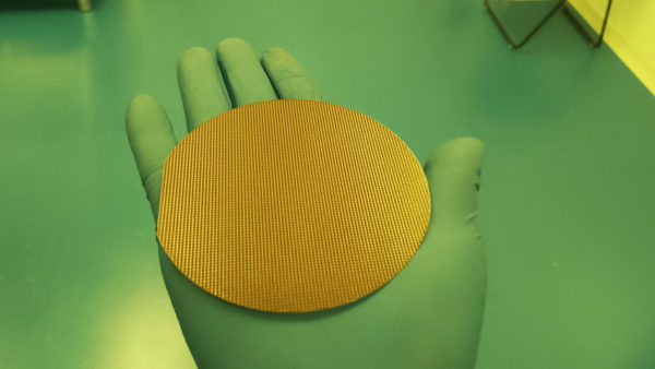
Gallium Oxide-Ga2O3
Gallium oxide single crystal material is the fourth-generation wide-bandgap semiconductor material after Si, SiC and GaN. Power devices based on β-Ga2O3 single crystal have higher breakdown voltage and lower on-resistance , so that it has lower conduction loss and higher power conversion efficiency, and has great application potential in power electronic devices. Gallium oxide is a new type of semiconductor crystal material from Japan, which can produce high-quality, large-scale single crystal substrates cheaply. It is expected to become the next generation of power device materials, and its potential exceeds gallium nitride and silicon carbide; The low-mismatch characteristics of GaN can be used for epitaxial substrates of GaN materials. Ga2O3 has an extremely wide bandgap of 4.9eV, exceeding the 3.3eV shown by SiC and GaN. This feature makes devices made of materials with narrower band gaps The devices formed are thinner, lighter, and can handle higher power. The wide bandgap allows operation at higher temperatures, thereby reducing the need for bulky cooling device systems. This difference enables Ga2O3 to withstand higher temperatures than silicon, SiC and GaN have larger electric fields without breakdown.
In addition, Ga2O3 can handle the same amount of voltage over a shorter distance, making it very valuable to produce smaller, more efficient high-power transistors. Ga2O3 looks ideal for use in power distribution systems for electric vehicle charging, or converters that send power from alternative sources like wind turbines to the grid. The advantage of Ga2O3 is also its potential as metal-oxide-semiconductor field-effect transistors (better known as MOSFETS). Traditionally, these tiny electronic switches are made of silicon and are used in laptops, smartphones and other electronics. For systems like EV charging stations, we need MOSFETS that can operate at higher power levels than silicon-based devices, and this is where Ga2O3 could be the solution. In microelectronic devices, the bandgap is the main factor determining the conductivity of materials. A substance with a wide bandgap is usually a non-conductive insulator, and a substance with a narrow bandgap is a semiconductor.
Ultrasonic spraying technology is used for semiconductor photoresist coating. Compared with traditional coating processes such as spin coating and dip coating, it has the advantages of high uniformity, good encapsulation of microstructures, and controllable coating area. In the past 10 years, it has been fully demonstrated that the 3D microstructure surface photoresist coating using ultrasonic spraying technology, the prepared photoresist coating is significantly higher than the traditional spin coating in terms of microstructure wrapping and uniformity Craft.
The ultrasonic spraying system can precisely control the flow rate, coating speed and deposition volume. Low-speed spray shaping defines atomized spray as a precise and controllable pattern to avoid excessive spray when producing a very thin and uniform layer. The ultrasonic spray system can control the thickness from sub-micron to more than 100 microns, and can coat any shape or size.
About Cheersonic
Cheersonic is the leading developer and manufacturer of ultrasonic coating systems for applying precise, thin film coatings to protect, strengthen or smooth surfaces on parts and components for the microelectronics/electronics, alternative energy, medical and industrial markets, including specialized glass applications in construction and automotive.
Our coating solutions are environmentally-friendly, efficient and highly reliable, and enable dramatic reductions in overspray, savings in raw material, water and energy usage and provide improved process repeatability, transfer efficiency, high uniformity and reduced emissions.
Chinese Website: Cheersonic Provides Professional Coating Solutions