
Cubic Boron Arsenide
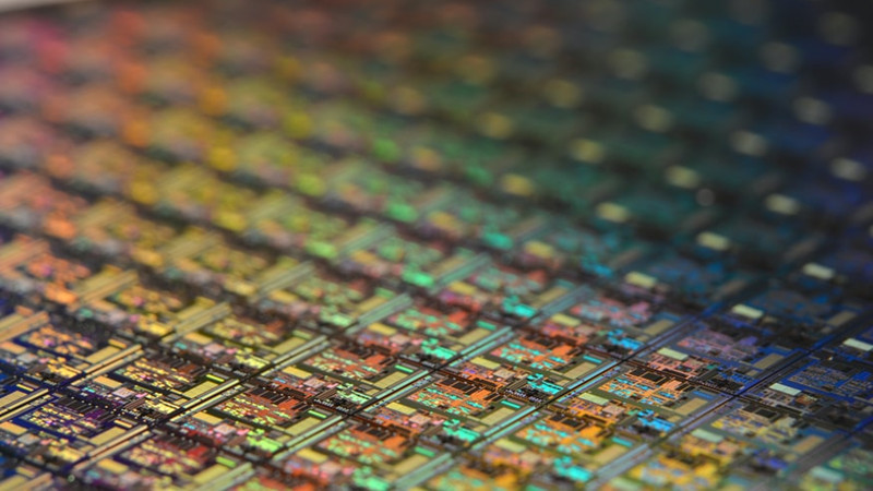
Cubic Boron Arsenide – Spray Photoresist Coating Onto MEMS Wafers – Cheersonic
A material called cubic boron arsenide overcomes two of the limitations of silicon as a semiconductor: it provides high mobility for electrons and holes, and it has good thermal conductivity.
It may be the best semiconductor material ever discovered, researchers say
As a semiconductor material, silicon still has shortcomings in its performance. Although electrons in silicon can easily pass through its structure, it has poor hole mobility. Other materials, such as gallium arsenide, which is widely used in lasers, also have good electron mobility, but not hole mobility. What’s more, silicon is not very good at conducting heat, so the chip temperature is always too hot.
Early experiments showed that the thermal conductivity of cubic boron arsenide is almost 10 times that of silicon. This is very attractive for heat dissipation. The study also proved that this material has a very good band gap, a property that makes it a great potential as a semiconductor material.
New research shows that boron arsenide possesses all the major qualities needed for an ideal semiconductor because of its high mobility of electrons and holes. This is important, the researchers noted, because in semiconductors, positive and negative charges are equal. Therefore, if a device is to be made, a material with less resistance to the movement of electrons and holes would be desirable.
Heat is the main bottleneck for many electronics today, and in major electric vehicle industries including Tesla, silicon carbide is replacing silicon as power electronics because it has 3 times the thermal conductivity of silicon, despite its electron migration rate is lower. The thermal conductivity of boron arsenide is 10 times that of silicon, and its mobility is also much higher than that of silicon, which could be a game changer.
So far, cubic boron arsenide has only been manufactured and tested on a laboratory scale, these products are not uniform, and more work is needed to determine whether cubic boron arsenide can be made in a practical, economical form. But the researchers say that in the near future, people may find some advantageous uses for the material, and its unique properties will make a big difference.
Ultrasonic spray has the advantages of precise and controllable spray flow rate, thin and uniform coating, and controllable spray range. It is very suitable for spraying electronic products and is increasingly used for research and production. Ultrasonic spray technology can be used to deposit a uniform coating on substrates of any width. Ultrasonic Spray Electronics technology enables these very thin coatings to be produced with extremely high uniformity, resulting in very accurate and repeatable results to enhance product functionality.