
Development of Mask
Development of Mask – Ultrasonic Coating System for Photoresist Deposition Offers Unique Advantages
Photolithography technology is a core step in semiconductor device manufacturing process, and lithography machine is also known as mask alignment exposure machine. This is because the commonly used lithography machine is mask alignment lithography. The optical lithography technology has roughly gone through three stages so far, and the mask plays an important role in the process of lithography exposure, and becomes more and more complex and fine with the development of lithography technology.
According to different mask exposure methods, it can be divided into contact exposure, proximity exposure and projection exposure. Since the 1990s, projection exposure lithography has become the mainstream of lithography technology. After that, when the technology node develops to 32nm, the optical characteristics of traditional lithography are limited by physical laws under very small size, and other auxiliary technologies must be used to continue to improve its resolution. These auxiliary technologies are mostly aimed at the improvement of mask. When the minimum linewidth is less than 28nm, multiple exposure technology is required to split the mask into multiple and expose them separately.
The rapid increase in the complexity and number of masks also increases the cost of mask manufacturing and maintenance. After entering the nanoscale, the cost and production cycle of masks have also increased significantly, and a large part of the cost expenditure in lithography is used for mask production.
There is a risk that maskless lithography technology will be replaced in the future. Therefore, in recent years, the industry has also started the research of maskless lithography technology, among which the representative technologies are: charged particle maskless lithography (CPML), optical maskless lithography (OML). It is worth noting that, at present, the flat panel display, semiconductor, touch and other industries around the world basically use mask as the reference pattern for exposure and mass production. The maskless lithography technology has low accuracy and efficiency, and is mainly used in the circuit board industry. With the progress of scientific research, it is not ruled out that the emergence of new maskless lithography technology will replace the original process technology, resulting in the risk of technology substitution.
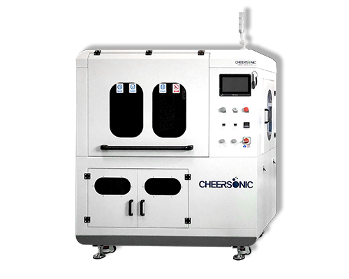
Ultrasonic spraying technology is used for semiconductor photoresist coating. Compared with traditional coating processes such as spin coating and dip coating, it has the advantages of high uniformity, good encapsulation of microstructures, and controllable coating area. In the past 10 years, it has been fully demonstrated that the 3D microstructure surface photoresist coating using ultrasonic spraying technology, the prepared photoresist coating is significantly higher than the traditional spin coating in terms of microstructure wrapping and uniformity Craft.
Chinese Website: Cheersonic Provides Professional Coating Solutions