
Introduction of Photoresist Classification
Introduction of Photoresist Classification – Deposit Photoresist – Cheersonic
1. Classification by application field
Photoresists are classified by application fields and can be divided into PCB photoresists, display panel photoresists, semiconductor photoresists and other photoresists.
In the PCB industry: the main photoresists used are dry film photoresist, wet film photoresist, photosensitive solder resist ink, etc. The dry film is pasted on the treated copper-clad plate with a special film for exposure and development; the wet-film and photoimageable solder resist inks are coated on the copper-clad plate, and then exposed and developed after drying. Dry film and wet film have their own advantages. Generally speaking, the resolution of wet film photoresist is higher than that of dry film, and the price is lower. Part of the market of dry film photoresist is being replaced.
In the flat panel display industry: the main photoresists used are color and black photoresists, LCD touch screen photoresists, TFT-LCD positive photoresists, etc. In the production process of photolithography and etching, photoresist is coated on the surface of the crystal film, and the pattern on the mask (mask) is transferred to the film after exposure, development and etching to form a pattern corresponding to the mask. geometric figures.
In the semiconductor integrated circuit manufacturing industry: g-line photoresist, i-line photoresist, KrF photoresist, ArF photoresist, etc. are mainly used. In the manufacturing process of large-scale integrated circuits, more than ten photolithography operations are generally performed on silicon wafers. In each photolithography and etching process, the photoresist must pass through pre-baking, gluing, pre-baking, alignment, exposure, post-baking, development and etching, etc. The graphics are transferred to the silicon wafer.
2. Classification by display effect
Photoresists can be divided into positive photoresists and negative photoresists.
①The pattern formed when the negative photoresist is developed is opposite to the mask (mask)
②The pattern formed by the positive photoresist is the same as that of the mask.
The production process of the two is basically the same, the difference is that the main raw materials are different.
3. According to chemical structure classification
Photoresists can be divided into photopolymerization type, photodecomposition type, photocrosslinking type and chemical amplification type.
① The photopolymerizable photoresist uses vinyl monomers to generate free radicals under the action of light, which further initiates the polymerization of monomers, and finally generates polymers;
(2) Photodecomposition type photoresist, using material containing diazoquinone compound (DQN) as a sensitizer, after being illuminated, a photolysis reaction occurs, which can be made into a positive photoresist;
③The photo-crosslinking photoresist uses polyvinyl alcohol laurate as photosensitive material. Under the action of light, an insoluble network structure is formed, which acts as a resist and can be made into negative photoresist. .
④Chemically amplified photoresist. After the semiconductor integrated circuit lithography technology began to use the deep ultraviolet (DUV) light source, the chemical amplification (CAR) technology gradually became the mainstream of the industry application. In chemically amplified photoresist technology, the resin is polyethylene protected by chemical groups and thus difficult to dissolve. Chemically amplified photoresists use photoacids (PAGs) as photoinitiators. When the photoresist is exposed, the photoacid agent (PAG) in the exposed areas will generate an acid. This acid acts as a catalyst during the post-heat bake process and will remove the resin’s protecting groups so that the resin becomes more soluble. The chemically amplified photoresist has 10 times the exposure speed of DQN photoresist, and has good optical sensitivity to deep ultraviolet light sources, as well as high contrast and high resolution.
4. Classification according to exposure wavelength
Photoresist can be divided into UV photoresist (300~450nm), deep UV photoresist (160~280nm), extreme ultraviolet photoresist (EUV, 13.5nm), electron beam photoresist, ion beam photoresist , X-ray photoresist, etc. Photoresists with different exposure wavelengths have different limit resolutions for photolithography. Generally speaking, the shorter the wavelength, the better the processing resolution when using the same process method.
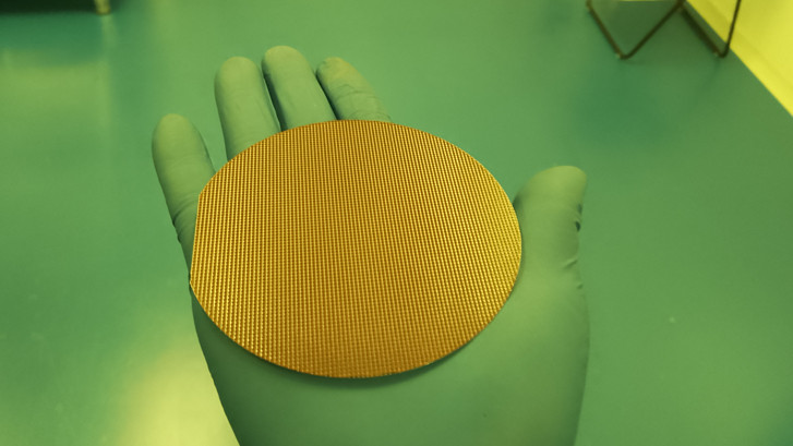
Ultrasonic spraying technology is used for semiconductor photoresist coating. Compared with traditional coating processes such as spin coating and dip coating, it has the advantages of high uniformity, good encapsulation of microstructures, and controllable coating area. In the past 10 years, it has been fully demonstrated that the 3D microstructure surface photoresist coating using ultrasonic spraying technology, the prepared photoresist coating is significantly higher than the traditional spin coating in terms of microstructure wrapping and uniformity Craft.
The ultrasonic spraying system can precisely control the flow rate, coating speed and deposition volume. Low-speed spray shaping defines atomized spray as a precise and controllable pattern to avoid excessive spray when producing a very thin and uniform layer. The ultrasonic spray system can control the thickness from sub-micron to more than 100 microns, and can coat any shape or size.