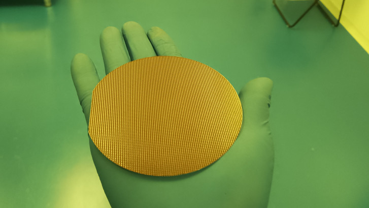
Reasons for tight 8-inch wafer production capacity
In the past few years, the production capacity of 8-inch wafers has been tight, mainly for the following reasons.
1. Driven by application requirements. On the application side, the strong demand for 8-inch wafer foundry mainly comes from power devices, power management ICs, image sensors, fingerprint recognition chips, and display driver ICs. Since analog/discrete devices have the characteristics of mature process + special process, most of these products will be produced on 8-inch or 6-inch lines.
Especially for power devices, the market demand for them has been quite strong in recent years, which has brought more business opportunities to the 8-inch wafer production line.
According to IC insights statistics, in terms of annual shipments of power devices, the compound annual growth rate from 2016 to 2021 will be 5.2%. In 2017, sales of power discrete devices increased by 10.4% year-on-year. Benefiting from the drive of automotive and industrial applications, it was expected that the power discrete device market would maintain a growth rate of around 5% in the next three years.
The demand for power devices in automotive electronics and industrial applications is greater than the supply, leading to price increases, and the demand for power devices for 8-inch wafer production capacity is greater than the supply, resulting in price increases for 8-inch wafers.
Second, the supply of equipment is insufficient. The market’s insufficient supply of equipment used in 8-inch fabs is also an important reason for the tight production capacity.
Since most 8-inch wafer foundries were established earlier, most of them have been operating for more than 10 years, and some equipment is too old or difficult to repair. At the same time, due to the huge capital expenditure of the current 12-inch wafer foundries, some manufacturers have stopped The 8-inch wafer production line has been established, making related equipment suppliers lack of enthusiasm for research and development and production of related equipment.
In recent years, the equipment needed for the expansion of 8-inch wafer foundry production capacity mainly comes from the second-hand market, among which etching machines, lithography machines, and measurement equipment are the most sought-after, and memory manufacturers upgrading from 8-inch to 12-inch have contributed to this market A lot, such as Samsung and Hynix. However, overall, the second-hand equipment market has limited resources and is gradually drying up.
3. 8-inch wafer foundry production lines are reduced. According to statistics, from 2008 to 2016, 37 8-inch wafer foundries were closed, and 15 factories were converted from 8-inch to 12-inch. As of 2016, the number of 8-inch wafer foundries in the world has decreased to 180. However, since 2016, the speed of 8-inch fab closures has slowed down, but the trend of reduction has not changed.
Traditional IDMs are reducing the scale of 8-inch wafer production lines and investing more resources in the construction and improvement of 12-inch production lines. This is mainly due to the increasingly fierce market competition. For IDMs, the investment in 8-inch production lines The output ratio is getting lower and lower, and the enthusiasm for large-scale operation of these production lines is no longer high. In addition to retaining a part of the necessary 8-inch wafer production lines, more and more 8-inch wafer processing tasks are outsourced to foundries . In this way, the production capacity of 8-inch wafers is objectively reduced.
The larger the wafer size, the higher the utilization efficiency. The 12-inch wafer has a larger usable area to achieve efficiency optimization. Compared with the 8-inch wafer, the 12-inch usable area is more than twice.
In recent years, TI has been steadily increasing its output of analog chips on 12-inch wafers to cut costs and improve production efficiency. TI said the 12-inch fab yields chips that are 40 percent cheaper than the 8-inch wafers used by competitors. Also, for analog purposes, the ROI of a 12-inch fab may be higher, as it can last 20-30 years.
Of course, the reasons for the tight production capacity of 8-inch wafers are not limited to the above three points, and the others will not be repeated here.
Ultrasonic spraying is a simple, economical and repeatable process for photoresist coating in lithographic wafer processing. Ultrasonic coating systems use advanced layering techniques to finely control flow rate, coating rate and deposition volume. Low velocity spray shaping defines the atomized spray as a precise, controlled pattern, avoiding overspray while producing a very thin, uniform layer. Direct spraying using ultrasonic technology has proven to be a reliable and effective method for depositing photoresist onto 3D microstructures, reducing equipment failures caused by over-exposure of metals to etchant.
About Cheersonic
Cheersonic is the leading developer and manufacturer of ultrasonic coating systems for applying precise, thin film coatings to protect, strengthen or smooth surfaces on parts and components for the microelectronics/electronics, alternative energy, medical and industrial markets, including specialized glass applications in construction and automotive.
Our coating solutions are environmentally-friendly, efficient and highly reliable, and enable dramatic reductions in overspray, savings in raw material, water and energy usage and provide improved process repeatability, transfer efficiency, high uniformity and reduced emissions.
Chinese Website: Cheersonic Provides Professional Coating Solutions

