
Semiconductor Interconnect
Semiconductor Interconnect – Semiconductor Coating Systems – Cheersonic
The conductivity of semiconductors lies between conductors and nonconductors (i.e. insulators), a property that allows us to fully control the flow of electricity. Components such as transistors can be built through wafer-based lithography, etching and deposition processes, but they also need to be connected to send and receive power and signals.
Metals are used for circuit interconnection because of their electrical conductivity. Metals used in semiconductors need to meet the following conditions:
Low resistivity: Since metal circuits need to carry current, the metals in them should have low resistance.
Thermochemical stability: The properties of the metal material must remain unchanged during the metal interconnection process.
· High reliability: With the development of integrated circuit technology, even a small amount of metal interconnect material must have sufficient durability.
· Manufacturing cost: Even if the first three conditions are met, if the material cost is too high, it cannot meet the needs of mass production.
The interconnect process mainly uses two substances, aluminum and copper.
①Aluminum interconnection process
The aluminum interconnect process begins with aluminum deposition, photoresist application, and exposure and development, followed by etching to selectively remove any excess aluminum and photoresist before proceeding to the oxidation process. After the aforementioned steps are completed, the photolithography, etching and deposition processes are repeated continuously until the interconnection is completed.
In addition to its excellent electrical conductivity, aluminum is also characterized by easy lithography, etching and deposition. In addition, it has a lower cost and better adhesion to the oxide film. The disadvantage is that it is easy to corrode and has a low melting point. In addition, to prevent the aluminum from reacting with the silicon causing connection problems, a metal deposit called a “barrier metal” is added to separate the aluminum from the wafer.
Aluminum circuits are formed by deposition. After the wafer enters the vacuum chamber, a thin film of aluminum particles adheres to the wafer. This process is called “Vapor Deposition (VD)” and includes both chemical vapor deposition and physical vapor deposition.
②Copper interconnection process
With the improvement of semiconductor process precision and the reduction of device size, the connection speed and electrical characteristics of aluminum circuits are gradually unable to meet the requirements. For this reason, we need to find new conductors that meet the requirements of both size and cost. The first reason why copper can replace aluminum is that it has lower resistance and therefore enables faster device connection speeds. Second, copper is more reliable because it is more resistant than aluminum to electromigration, which is the movement of metal ions that occurs when an electric current flows through the metal.
However, copper does not easily form compounds, so it is difficult to vaporize and remove it from the wafer surface. In response to this problem, we no longer etch copper, but deposit and etch dielectric material, so that metal circuit patterns consisting of channels and via holes can be formed where needed, and then copper is filled into the aforementioned “” pattern” to achieve interconnection, and the final filling process is called “damascene process”.
As the copper atoms continue to diffuse into the dielectric, the latter becomes less insulating and creates a barrier that blocks further copper atoms from diffusing. A thin copper seed layer is then formed on the barrier layer. After this step, electroplating can be performed, that is, the high aspect ratio pattern is filled with copper. After filling, the excess copper can be removed by metal chemical mechanical polishing (CMP) method, and the oxide film can be deposited after completion, and the excess film can be removed by photolithography and etching process. The entire process described above needs to be repeated until the copper interconnection is completed.
As can be seen from the above comparison, the difference between copper interconnects and aluminum interconnects is that the excess copper is removed by metal CMP rather than etching.
Ultrasonic spraying technology is used for semiconductor photoresist coating. Compared with traditional coating processes such as spin coating and dip coating, it has the advantages of high uniformity, good encapsulation of microstructures, and controllable coating area. In the past 10 years, it has been fully demonstrated that the 3D microstructure surface photoresist coating using ultrasonic spraying technology, the prepared photoresist coating is significantly higher than the traditional spin coating in terms of microstructure wrapping and uniformity Craft.
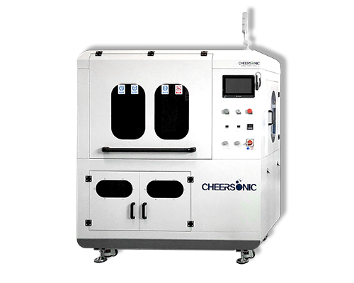
The ultrasonic spraying system can precisely control the flow rate, coating speed and deposition volume. Low-speed spray shaping defines atomized spray as a precise and controllable pattern to avoid excessive spray when producing a very thin and uniform layer. The ultrasonic spray system can control the thickness from sub-micron to more than 100 microns, and can coat any shape or size.