
Semiconductor Packaging
Semiconductor Packaging – Semiconductor Coating Systems – Cheersonic
A wafer that has been processed through the previous processes results in square chips of equal size (also known as “single wafers”). The next thing to do is to get the individual chips by dicing. Freshly cut chips are fragile and cannot exchange electrical signals, and need to be handled separately. This process is encapsulation, which involves forming a protective casing around the semiconductor chips and enabling them to exchange electrical signals with the outside world. The entire packaging process is divided into five steps, namely wafer sawing, single die attach, interconnection, molding and package testing.
01 Wafer sawing
To cut countless densely packed chips from a wafer, we first carefully “grind” the backside of the wafer until it is thick enough for the packaging process. After grinding, we can cut along the scribe lines on the wafer until the semiconductor chips are separated.
There are three wafer sawing techniques: blade cutting, laser cutting and plasma cutting. Blade dicing refers to cutting wafers with diamond blades, which is prone to frictional heat and debris that can damage the wafer. Laser cutting is more precise and can easily handle wafers with thin thicknesses or small scribe line spacing. Plasma dicing uses the principle of plasma etching, so even if the scribe line spacing is very small, this technique can also be used.
02 Single Wafer Attachment
After all the chips are separated from the wafer, we need to attach the individual chips (single wafers) to the substrate (lead frame). The role of the substrate is to protect the semiconductor chips and allow them to exchange electrical signals with external circuits. A liquid or solid tape adhesive can be used to attach the chip.
03 Interconnect
After attaching the chip to the substrate, we also need to connect the contact points of the two in order to exchange electrical signals. There are two connection methods that can be used in this step: wire bonding using thin metal wires and flip chip bonding using ball gold or tin bumps. Wire bonding is a traditional method, and flip-chip bonding technology can speed up semiconductor manufacturing.
04 Forming
After the connection of the semiconductor chips is completed, it is necessary to use a molding process to add a package to the outside of the chips to protect the semiconductor integrated circuits from external conditions such as temperature and humidity. Once the encapsulation mold is made as required, we place both the semiconductor chip and epoxy molding compound (EMC) into the mold and seal it. The sealed chip is in its final form.
05 Package test
Chips that already have their final form go through a final defect test. All that goes into final testing are finished semiconductor chips. They will be put into test equipment and set different conditions such as voltage, temperature and humidity for electrical, functional and speed tests. The results of these tests can be used to find defects, improve product quality and production efficiency.
Evolution of Packaging Technology
Packaging has undergone several technological innovations over the past few years as chip size has decreased and performance requirements have increased. Some future-oriented packaging technologies and solutions include the use of deposition for traditional back-end processes such as wafer-level packaging (WLP), bumping and redistribution layer (RDL) technologies, and lithography for front-end wafer fabrication. Etching and cleaning techniques.
What is advanced packaging?
Traditional packaging requires each chip to be cut from a wafer and placed into a mold. Wafer-level packaging (WLP) is a type of advanced packaging technology that refers to the direct packaging of chips that are still on a wafer. The process of WLP is to first package and test, and then all the formed chips are separated from the wafer at one time. The advantage of WLP is lower production cost compared to traditional packaging.
Advanced packaging can be divided into 2D packaging, 2.5D packaging and 3D packaging.
Smaller 2D package
As mentioned earlier, the main uses of the packaging process include sending signals from the semiconductor chip to the outside, and the bumps formed on the wafer are the contact points for sending input/output signals. These bumps are divided into two types: fan-in and fan-out. The fan shape of the former is inside the chip, and the fan shape of the latter is beyond the scope of the chip. We refer to the input/output signal as I/O (input/output) and the number of input/output as the I/O count. The I/O count is an important basis for determining the packaging method. Fan-in packaging is used if the I/O count is low. Since the chip size does not change much after packaging, this process is also known as chip-scale packaging (CSP) or wafer-level chip-scale packaging (WLCSP). If the I/O count is high, a fan-out packaging process is often used, and a redistribution layer (RDL) is required in addition to the bumps for signaling. This is “Fan-Out Wafer Level Packaging (FOWLP)”.
2.5D package
2.5D packaging technology can put two or more types of chips into a single package while allowing signals to travel laterally, which can increase the size and performance of the package. The most widely used 2.5D packaging method is to put memory and logic chips into a single package through a silicon interposer. 2.5D packaging requires core technologies such as through-silicon vias (TSV), micro-bumps, and fine-pitch RDL.
3D packaging
3D packaging technology can place two or more types of chips into a single package while allowing signals to travel vertically. This technique is suitable for smaller and higher I/O count semiconductor chips. TSV can be used for chips with high I/O counts, wire bonding can be used for chips with low I/O counts, and finally a signal system with chips arranged vertically. The core technologies required for 3D packaging include TSV and microbump technology.
Ultrasonic spraying technology is used for semiconductor photoresist coating. Compared with traditional coating processes such as spin coating and dip coating, it has the advantages of high uniformity, good encapsulation of microstructures, and controllable coating area. In the past 10 years, it has been fully demonstrated that the 3D microstructure surface photoresist coating using ultrasonic spraying technology, the prepared photoresist coating is significantly higher than the traditional spin coating in terms of microstructure wrapping and uniformity Craft.
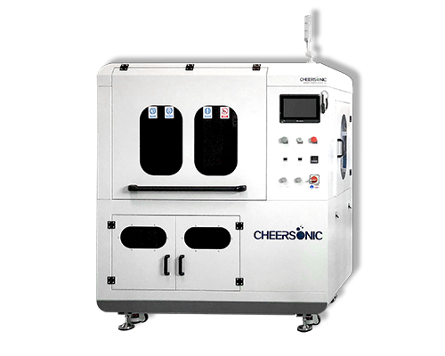
The ultrasonic spraying system can precisely control the flow rate, coating speed and deposition volume. Low-speed spray shaping defines atomized spray as a precise and controllable pattern to avoid excessive spray when producing a very thin and uniform layer. The ultrasonic spray system can control the thickness from sub-micron to more than 100 microns, and can coat any shape or size.