
Semiconductor Process Masks And Pellicle Films
Semiconductor Process Masks And Pellicle Films – Electronics Coating – Cheersonic
Reticles and Dust Films:
Mask: The pattern transfer master in the microelectronics manufacturing process of the mask. The function of the mask is to transfer the designer’s circuit pattern to the substrate or wafer in the downstream industry by exposure, so as to achieve mass production . As the benchmark and blueprint for lithographic reproduction patterns, the mask is the key to connecting industrial design and process manufacturing. The precision and quality level of the mask will directly affect the quality rate of the final downstream products.
Mask substrate material: synthetic quartz is the main material, and the raw materials are mainly imported;
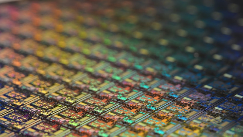
Photolithography is to precisely transfer the pattern on the mask to the photoresist, so if there is a defect on the mask, it will all be transferred to the photoresist. The mask is made of chromium (Cr) as a light-shielding material on a transparent quartz substrate to form a certain pattern. Defects, scratches, dust, or particles in the chromium film can cause patterning defects and reduce the yield of semiconductor devices. The manufacturing, inspection and management of masks are important topics in the front-end production line.
With the development of miniaturization, the structure of masks such as phase shift masks and OPCs has also become more and more complex.
Phase Shift Mask (PSM, Phase Shift Mask): On the mask, periodically in adjacent patterns, every other pattern feature changes the structure (thinning or thickening) of the mask, so that the The phase difference of adjacent patterns is 180 degrees, so that the purpose of improving the resolution can be achieved.
The phase-shift mask technology greatly increases the manufacturing difficulty and cost of the mask.
OPC (Optical Proximity Effect Correction) abbreviation, optical proximity effect correction. During the exposure process, the quality of the final image is often degraded due to the optical proximity effect: the change of the line width; the rounding of the corners; the shortening of the line length, etc. Therefore, it is necessary to form an auxiliary pattern for correcting the pattern on the reticle to reduce the proximity effect of the light and improve the resolution.
Dust film:
The dust-proof film is a film to prevent the particles on the optical mask from causing graphic defects. At a position of a few mm on the mask, a thin transparent film is pasted on the frame, so that even if there are particles, the dust-proof film It will also not affect the exposure graphics. Because the mask is separated from the dustproof film, the distance between the protective film and the substrate is generally 6 mm, and the focal depth of the lithography machine is at most 100~200 nm. When the particles are projected on the wafer surface, they will be defocused. A blurred image is formed on the wafer surface, which has little effect on wafer surface stripes.
The ultrasonic coating system can use advanced layering technology to precisely control the flow rate, coating speed and deposition amount. Low-speed spray forming defines an atomizing spray as a precise, controllable pattern, avoiding excessive spraying when producing very thin and uniform layers. It turns out that direct spraying using ultrasonic technology is a reliable and effective way to deposit photoresist on 3D microstructures, thereby reducing equipment failures caused by excessive metal exposure to etchant.
Ultrasonic spray systems have proven to be suitable for a variety of applications that require uniform, repeatable photoresist or polyimide film coatings. Cheersonic’s coating system can control thicknesses from sub-micron to more than 100 microns, and can coat any shape or size. It is a feasible alternative to other coating technologies such as spin coating and traditional spray coating.
Cheersonic’s non-blocking ultrasonic coating technology is known for its ultra-thin micron-layer coatings of functional and protective materials. The ultrasonic vibration of the nozzle effectively dispersed the particles in the suspension and produced a very uniform particle dispersion in the film layer, while the conductive particles did not settle out of the suspension.