
Semiconductor Testing
Semiconductor Testing – Semiconductor Coating Systems – Cheersonic
The main goal of the test is to check whether the quality of the semiconductor chip reaches a certain standard, thereby eliminating defective products and improving the reliability of the chip. In addition, tested defective products do not enter the packaging step, helping to save cost and time. Electronic Die Sorting (EDS) is one test method for wafers.
EDS is a process that inspects the electrical characteristics of individual chips in wafer state and thereby improves semiconductor yield. EDS can be divided into five steps, as follows:
01 Electrical parameter monitoring (EPM)
EPM is the first step in semiconductor chip testing. This step will test every device (including transistors, capacitors, and diodes) that a semiconductor integrated circuit needs to use to ensure that its electrical parameters are up to standard. The primary role of EPM is to provide measured electrical characteristic data that will be used to improve the efficiency of the semiconductor manufacturing process and product performance (not to detect defective products).
02 Wafer burn-in test
The semiconductor defect rate comes from two aspects, namely the rate of manufacturing defects (higher in the early stage) and the rate of defects occurring throughout the life cycle thereafter. Wafer burn-in test refers to the testing of wafers under a certain temperature and AC/DC voltage to find out products that may be defective at an early stage, that is, to improve the reliability of the final product by discovering potential defects .
03 Detection
After the burn-in test is completed, a probe card is used to connect the semiconductor chip to the test equipment, after which the wafer can be tested for temperature, speed and motion to verify the relevant semiconductor functions. See the table for a description of the specific test steps.
04 Patch
Patching is the most important test step, because some bad chips can be repaired by simply replacing the faulty component.
05 Ink
Chips that fail electrical tests have already been sorted out in previous steps, but need to be marked to distinguish them. Whereas in the past we needed to mark defective chips with special inks to ensure they were identifiable with the naked eye, today the system automatically sorts them based on test data values.
Ultrasonic spraying technology is used for semiconductor photoresist coating. Compared with traditional coating processes such as spin coating and dip coating, it has the advantages of high uniformity, good encapsulation of microstructures, and controllable coating area. In the past 10 years, it has been fully demonstrated that the 3D microstructure surface photoresist coating using ultrasonic spraying technology, the prepared photoresist coating is significantly higher than the traditional spin coating in terms of microstructure wrapping and uniformity Craft.
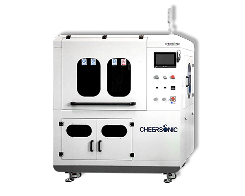
The ultrasonic spraying system can precisely control the flow rate, coating speed and deposition volume. Low-speed spray shaping defines atomized spray as a precise and controllable pattern to avoid excessive spray when producing a very thin and uniform layer. The ultrasonic spray system can control the thickness from sub-micron to more than 100 microns, and can coat any shape or size.