
SiC Power Module Package Form
With the development of emerging strategic industries, the application requirements of the third generation wide bandgap power semiconductor silicon carbide materials and chips, the module packaging technology at home and abroad has also developed rapidly, and the pursuit of packaging technology with low stray parameters and small size has become a close focus of packaging. Focus, domestic and foreign scientific research teams and the semiconductor industry have designed high-performance power modules with different structures to improve the performance of SiC-based controllers.
(1) Traditional packaging: Manufacturers such as Wolfspeed, Rohm, and Semikron mostly continue to use traditional Si-based packaging methods, which have low power levels, contain metal bonding wires, and have large stray inductance.
(2) DBC+PCB hybrid packaging: Cha et al. and Seal et al. integrated DBC and PCB boards, connected chips and PCB boards through bonding wires, and developed DBC+PCB hybrid packaging. The commutation circuit is directly controlled between PCB layers, and the commutation path is reduced to reduce parasitic inductance.
(3) SKiN package: German Semikron company adopts nano-silver sintering and SKiN wiring technology, and uses flexible PCB board instead of bonding wire to realize the electrical connection of the upper and lower surfaces of the chip, and the parasitic inductance of the internal circuit of the module is only 1. 5 nH.
(4) Planar interconnect package: By eliminating metal bonding wires, the current loop is expanded from the DBC board plane layout to the interlayer layout of the upper and lower planes of the chip, which significantly reduces the loop area and stray inductance parameters, such as Silicon Power The company adopts direct terminal connection (DLB), IR’s Cu-Clip IGBT and Siemens’ SiPLIT technology, etc.
(5) Double-sided welding (sintering) packaging: Weld DBC heat dissipation substrates on both sides of the power chip to provide heat dissipation channels for the upper and lower surfaces of the chip; or use silver sintering technology to weld DBC on one side of the chip and connect the aluminum sheet on the other side. Double-sided heat dissipation can not only optimize the edge field strength of the substrate, but also reduce electromagnetic interference (EMI), reduce the parasitic capacitance of the midpoint of the bridge arm to the ground, and make it have the advantages of low loss, good thermal performance, and low manufacturing cost. Oak Ridge Laboratory, CRRC Times Electric, Tianjin University and CPES can reduce the parasitic inductance to 5 nH. At the same time, copper sintering, as a lower-cost chip connection solution, is regarded as a research hotspot in the next few years. At present, the double-sided heat dissipation technology is mainly used in the internal modules of new energy electric vehicles.
(6) Crimping package: The interface of each layer of the crimping device relies on pressure contact to realize electric heat conduction, which is divided into two types: boss type and spring type. Compared with soldered devices, crimped package structure modules have the advantages of high power density, double-sided heat dissipation, low on-state loss, strong impact resistance, resistance to failure short circuit, and easy series connection, etc., and use a smaller number of crimped modules It can meet the voltage level and capacity requirements during commutation, but due to sealing and other requirements, LTCC ceramic design is often used, the cost is high, and the crimping package structure is complicated. Currently, it is only used in the manufacture of high-voltage modules and has a certain application market. But there is still a certain gap from the actual application in the automotive field.
(7) Three-dimensional (3D) packaging: Tokuyama et al. and Herbsommer et al. superimposed the upper bridge arm of the SiC module directly on the lower bridge arm. Since the structure of the SiC module is vertical, the physical length of the commutation circuit can be greatly shortened to further Reduce di/dt related problems.
At present, the biggest advantage of this packaging technology is that it can reduce the parasitic inductance of the module to less than 1 nH. In addition, the terminal with the largest voltage fluctuation is placed in the middle of the three-dimensional sandwich structure, so that the parasitic capacitance between the terminal and the heat sink is drastically reduced, thereby suppressing the electromagnetic interference noise.
Ultrasonic spraying technology is used for semiconductor photoresist coating. Compared with traditional coating processes such as spin coating and dip coating, it has the advantages of high uniformity, good encapsulation of microstructures, and controllable coating area. In the past 10 years, it has been fully demonstrated that the 3D microstructure surface photoresist coating using ultrasonic spraying technology, the prepared photoresist coating is significantly higher than the traditional spin coating in terms of microstructure wrapping and uniformity Craft.
The ultrasonic spraying system can precisely control the flow rate, coating speed and deposition volume. Low-speed spray shaping defines atomized spray as a precise and controllable pattern to avoid excessive spray when producing a very thin and uniform layer. The ultrasonic spray system can control the thickness from sub-micron to more than 100 microns, and can coat any shape or size.
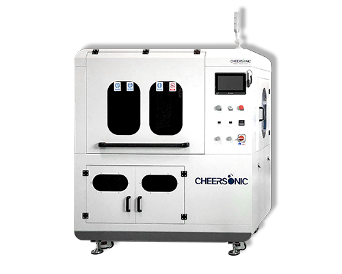
About Cheersonic
Cheersonic is the leading developer and manufacturer of ultrasonic coating systems for applying precise, thin film coatings to protect, strengthen or smooth surfaces on parts and components for the microelectronics/electronics, alternative energy, medical and industrial markets, including specialized glass applications in construction and automotive.
Our coating solutions are environmentally-friendly, efficient and highly reliable, and enable dramatic reductions in overspray, savings in raw material, water and energy usage and provide improved process repeatability, transfer efficiency, high uniformity and reduced emissions.
Chinese Website: Cheersonic Provides Professional Coating Solutions