Silicon Carbide Preparation Process
Silicon Carbide Preparation Process – Circuit Board Spray – Cheersonic
The first step is to generate raw materials, mix high-purity silicon powder and high-purity carbon powder uniformly according to the process formula, and pass a specific reaction process in the reaction chamber under high temperature conditions above 2,000°C to remove the residual and reaction powder surface in the reaction environment The adsorbed trace impurities make the silicon powder and carbon powder react according to the predetermined stoichiometric ratio to synthesize silicon carbide particles of specific crystal form and particle size. After crushing, screening, cleaning and other processes, high-purity silicon carbide powder raw materials that meet the crystal growth requirements are obtained.

The second crystal growth is to heat the silicon carbide powder at a high temperature above 2,300°C and a low pressure close to vacuum to sublimate it to produce a reaction gas containing Si, Si2C, SiC2 and other gas phase components, and produce silicon carbide through solid-gas reaction Single crystal reaction source; due to the difference in the gas phase partial pressure of Si and C components formed by the solid phase sublimation reaction, the Si/C stoichiometric ratio varies with the thermal field distribution, and the gas phase components need to be distributed according to the designed thermal field and temperature gradient and transport, so that the components are transported to the predetermined crystallization position in the growth chamber;
The third crystal ingot processing The silicon carbide crystal ingot is oriented using an X-ray single crystal orienter, and then ground and rounded by precision machining, and processed into a silicon carbide crystal rod with a standard diameter and angle. Check the dimensions, angles and other indicators of all formed crystal ingots.
The fourth crystal ingot cutting, under the premise of considering the follow-up processing allowance, uses diamond thin wire to cut silicon carbide crystal ingots into different thicknesses that meet customer needs, and uses fully automatic testing equipment for warp (Warp), bending Bow, thickness change (TTV) and other surface type detection.
The fifth cutting disc grinding is to thin the cutting disc to the corresponding thickness through the grinding liquid formulated by its own process, and eliminate the line marks and damage on the surface. Use automatic testing equipment and non-contact resistivity tester to test the surface shape and electrical properties of all cut pieces.
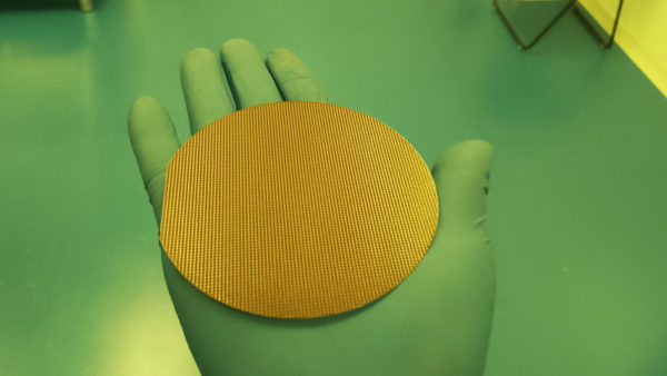
Sixth polishing of abrasive discs: Mechanical polishing and chemical polishing are performed on the abrasive discs with a well-proportioned polishing solution to eliminate surface scratches, reduce surface roughness and eliminate processing stress, etc., so that the surface of the abrasive discs can reach nano-level flatness. Use X-ray diffractometer, atomic force microscope, surface flatness tester, surface defect comprehensive tester and other equipment to detect various parameters and indexes of silicon carbide polished wafers, and judge the quality level of polished wafers accordingly.
The seventh polishing piece is cleaned in a class 100 ultra-clean room. The polishing piece in the cleaning machine is cleaned with a specific ratio of chemical reagents and deionized water to remove dust particles, metal ions, and organic contaminants on the surface of the polishing piece. etc., dried and packaged in a clean chip box to form a silicon carbide substrate that can be used by customers out of the box.
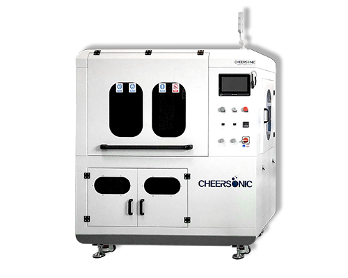
Ultrasonic spraying technology is used for semiconductor photoresist coating. Compared with traditional coating processes such as spin coating and dip coating, it has the advantages of high uniformity, good encapsulation of microstructures, and controllable coating area. In the past 10 years, it has been fully demonstrated that the 3D microstructure surface photoresist coating using ultrasonic spraying technology, the prepared photoresist coating is significantly higher than the traditional spin coating in terms of microstructure wrapping and uniformity Craft.
The ultrasonic spraying system can precisely control the flow rate, coating speed and deposition volume. Low-speed spray shaping defines atomized spray as a precise and controllable pattern to avoid excessive spray when producing a very thin and uniform layer. The ultrasonic spray system can control the thickness from sub-micron to more than 100 microns, and can coat any shape or size.
About Cheersonic
Cheersonic is the leading developer and manufacturer of ultrasonic coating systems for applying precise, thin film coatings to protect, strengthen or smooth surfaces on parts and components for the microelectronics/electronics, alternative energy, medical and industrial markets, including specialized glass applications in construction and automotive.
Our coating solutions are environmentally-friendly, efficient and highly reliable, and enable dramatic reductions in overspray, savings in raw material, water and energy usage and provide improved process repeatability, transfer efficiency, high uniformity and reduced emissions.
Chinese Website: Cheersonic Provides Professional Coating Solutions

