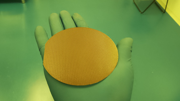
Spray Coating Photoresist On Silicon Wafers
Spray Coating Photoresist On Silicon Wafers – Ultrasonic Photoresist Coater – Cheersonic
Spin coating of photoresist, although an established technique for resist depositionis often not suitable for applications with high topography on the silicon or glasssurface. Since 3D structures such as trenches, V-grooves and holes are basic elementsin building the required functionality of MEMS devices, spin coating usually causesdefects on the resist layer. Especially in sidewall of trench, due to the gravity, the photoresist will flow down along the slope, accumulate at the bottom corner andcause the disconnection at the top corner. For metal patterning (metalized via-holes) the discontinuity of the photoresist layer in these regions iscritical. In a positive photolithography the metal layer will not be protected by the photoresist in the top corner regions. As a result the metal layer will be etchand the functionality of the device is affected. Another problem associated with thespinning process on the wafer with high topography is related to the uniformity of thedeposition. Due to the non-planarity of the wafer the uniformityof the photoresist layer on the top surface of the wafer is very poor.

As photoresist coating of high topography surfaces is basic in MEMS applications,recent efforts for the development in ultrasonic photoresist coating were discussed. As this ultrasonic photoresist coating approach is economical, simple and reproducible, this approach can potentially substitute conventional spin coating techniques and other methods. The ultrasonic photoresist spray method is a reliable method to improve the quality of the photoresist coating, not only on the flat surface, but also on the edges and sides of the slope within the trench.
Chinese Website: Cheersonic Provides Professional Coating Solutions
