
Technical characteristics of micromachining process
Silicon micromachining technology is developed from semiconductor integrated circuit technology. First of all, it draws on the mature microfabrication technology in the integrated circuit process, such as: photolithography, diffusion, ion implantation, epitaxy and film deposition. In addition, after more than 20 years of development, silicon micromachining technology has formed its own characteristics. Unlike the planar technology of integrated circuits, micromachining is basically a bulk processing technology, emphasizing the processing of silicon in the depth direction. . To sum up, the main contents of silicon micromachining technology are as follows:
1. Wet etching and dry etching of silicon
The etching technology of silicon is mainly used to process the precise three-dimensional structure or two-dimensional structure of the microsensor. Among them, wet etching includes anisotropic etching technology and isotropic etching technology of silicon; dry etching mainly includes: plasma Etching, laser etching (laser processing), LIGA technology (photolithography electroplating molding) and SLIGA technology (sacrificial layer photolithography electroplating molding technology), etc.
2. Silicon-on-insulator (SOI)
Silicon micromechanical sensors are generally composed of two parts: the sensitive device part and the integrated circuit part. Among them, the sensitive part is usually in contact with the measured environment, sometimes it is a harsh measured environment, and the integrated circuit part is most afraid of environmental pollution. Therefore, in order to ensure the working reliability and life of the sensor, the sensitive part and the integrated circuit part must be separated At this time, SOI is the most ideal separation material, which separates the two parts of the sensor on the silicon wafers on both sides of the SOI, perfectly realizing the integration of sensitive devices and integrated circuits.
3. Self-stop corrosion technology
The purpose of silicon micromachining is to form precise microstructures. In order to make the microstructures have consistent dimensions and properties, it is necessary to precisely control the etching depth, so self-stop etching technology must be used. Commonly used self-stop corrosion techniques include: p+ self-stop corrosion technology, including heavy doping and light doping; electrical passivation p-n junction self-stop corrosion technology; buried layer corrosion stop method, the most commonly used is SOI Method for self-stopping corrosion of structures.
4. Sacrificial layer technology
The sacrificial layer technology is used in the surface micromachining of silicon. Using this selective etching technology, the required micromechanical components can be obtained on the silicon surface. In the processing of silicon micromechanical sensors, the most commonly used sacrificial layer material is SiO2.
5. Keys and techniques
Key and technology are used to reliably connect separately fabricated micromechanical components together, so that complex micromechanical sensor structures can be obtained; on the other hand, key and technology are also used in the packaging of sensors. At present, there are mainly two bonding technologies, namely: electrostatic bonding and silicon-silicon direct bonding technology. Electrostatic bonding and technology adopt high-voltage electrostatic method, which can firmly combine silicon with glass, metal, alloy and other materials without any adhesive. This bond and technology is usually used in the packaging of sensors and integrated circuits, and its bonds and defects are: when the temperature changes, thermal stress is generated on the bond and surface due to the different thermal expansion coefficients between the bond and the material; silicon-silicon The direct bonding technology adopts the method of high temperature treatment, which can directly bond two silicon wafers together without any adhesive or electric field in the middle. This bond and technology is mostly used to combine several silicon micro-mechanical components into a complex micro-mechanical structure to realize silicon integrated packaging, and this packaging does not have the thermal stress of the package introduced by the different thermal expansion coefficients.
Cheersonic ultrasonic coating systems are used to spray thin films of polymers, conductive nanoparticles, or other functional materials used in sensors manufacturing. These conductive nanocoatings are used for applications such as biometrics security and medical device applications, as well as sensors designed for a variety of other applications.
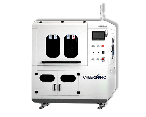
About Cheersonic
Cheersonic is the leading developer and manufacturer of ultrasonic coating systems for applying precise, thin film coatings to protect, strengthen or smooth surfaces on parts and components for the microelectronics/electronics, alternative energy, medical and industrial markets, including specialized glass applications in construction and automotive.
Our coating solutions are environmentally-friendly, efficient and highly reliable, and enable dramatic reductions in overspray, savings in raw material, water and energy usage and provide improved process repeatability, transfer efficiency, high uniformity and reduced emissions.
Chinese Website: Cheersonic Provides Professional Coating Solutions