
Wafer Lithography
Wafer Lithography – Polyimide Coatings – Photoresist Coating – Cheersonic
Lithography is the “printing” of a circuit pattern onto a wafer by light, which we can understand as drawing the plan on the surface of the wafer required for semiconductor fabrication. The higher the fineness of the circuit pattern, the higher the integration of the finished chip, which must be achieved through advanced lithography technology. Specifically, photolithography can be divided into three steps: coating photoresist, exposing and developing.
①Coating
Photoresist The first step in drawing circuits on a wafer is to apply photoresist over the oxide layer. Photoresist turns the wafer into “photo paper” by changing its chemical properties. The thinner the photoresist layer on the wafer surface, the more uniform the coating, the finer the pattern that can be printed. A “spin coating” method can be used for this step. According to the difference of light (ultraviolet) reactivity, photoresist can be divided into two types: positive and negative, the former will decompose and disappear after being exposed to light, leaving the pattern of the unilluminated area, while the latter will polymerize after being exposed to light. And let the graphics of the light-receiving part appear.
②Exposure
After the wafer is covered with a film of photoresist, the circuit can be printed by controlling the exposure of light, a process called “exposure.” We can selectively pass light through the exposure equipment, and when the light passes through the mask containing the circuit pattern, the circuit can be printed on the wafer with the photoresist film coated underneath.
During the exposure process, the finer the print pattern, the more components the final chip can accommodate, which helps improve production efficiency and reduce the cost of individual components. In this area, a new technology that is currently attracting attention is EUV lithography.
③Development
The step after exposure is to spray developer on the wafer to remove the photoresist from the areas not covered by the pattern, allowing the printed circuit pattern to emerge. After the development is completed, it needs to be checked through various measuring equipment and optical microscopes to ensure the quality of the circuit diagrams.
Ultrasonic spraying technology is used for semiconductor photoresist coating. Compared with traditional coating processes such as spin coating and dip coating, it has the advantages of high uniformity, good encapsulation of microstructures, and controllable coating area. In the past 10 years, it has been fully demonstrated that the 3D microstructure surface photoresist coating using ultrasonic spraying technology, the prepared photoresist coating is significantly higher than the traditional spin coating in terms of microstructure wrapping and uniformity Craft.
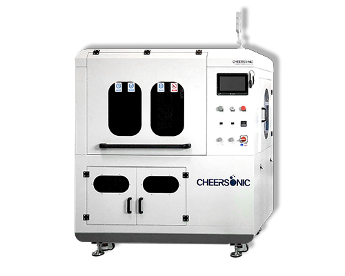
The ultrasonic spraying system can precisely control the flow rate, coating speed and deposition volume. Low-speed spray shaping defines atomized spray as a precise and controllable pattern to avoid excessive spray when producing a very thin and uniform layer. The ultrasonic spray system can control the thickness from sub-micron to more than 100 microns, and can coat any shape or size.