
Wafer Thin Film Deposition
Wafer Thin Film Deposition – Photoresist Coating – Cheersonic
To create the tiny devices inside the chip, we need to continuously deposit layers of thin films and etch away the excess, as well as add materials to separate the different devices. Each transistor or memory cell is built step-by-step through the above process. By “thin film” we mean here a “film” that is less than 1 micrometer (μm, millionth of a meter) thick and cannot be fabricated by ordinary machining methods. The process of placing a thin film containing the desired molecular or atomic unit onto a wafer is called “deposition.”
To form a multi-layer semiconductor structure, we need to fabricate a device stack, that is, alternately stack multiple layers of thin metal (conducting) films and dielectric (insulating) films on the surface of the wafer, and then repeat the etching process to remove excess parts and form a three-dimensional structure. The techniques that can be used in the deposition process include chemical vapor deposition (CVD), atomic layer deposition (ALD), and physical vapor deposition (PVD), which can be divided into dry and wet deposition methods.
①Chemical vapor deposition
In chemical vapor deposition, the precursor gases chemically react in the reaction chamber and produce films that adhere to the wafer surface and by-products that are pumped out of the chamber. Plasma-enhanced chemical vapor deposition requires the use of plasma to generate reactive gases. This approach lowers the reaction temperature and is therefore ideal for temperature-sensitive structures. Using plasma also reduces deposition times, often resulting in higher quality films.
②Atomic layer deposition
Atomic layer deposition forms thin films by depositing only a few atomic layers at a time. The key to the method is to cycle through individual steps in a certain order and maintain good control. Coating the precursor on the surface of the wafer is the first step, and then introducing different gases to react with the precursor can form the desired substance on the surface of the wafer.
③ Physical vapor deposition
As the name suggests, physical vapor deposition refers to the formation of thin films by physical means. Sputtering is a physical vapor deposition method, the principle of which is to sputter the atoms of the target material through the bombardment of argon plasma and deposit them on the surface of the wafer to form a thin film. In some cases, the deposited film can be treated and improved with techniques such as ultraviolet thermal processing (UVTP).
Ultrasonic spraying technology is used for semiconductor photoresist coating. Compared with traditional coating processes such as spin coating and dip coating, it has the advantages of high uniformity, good encapsulation of microstructures, and controllable coating area. In the past 10 years, it has been fully demonstrated that the 3D microstructure surface photoresist coating using ultrasonic spraying technology, the prepared photoresist coating is significantly higher than the traditional spin coating in terms of microstructure wrapping and uniformity Craft.
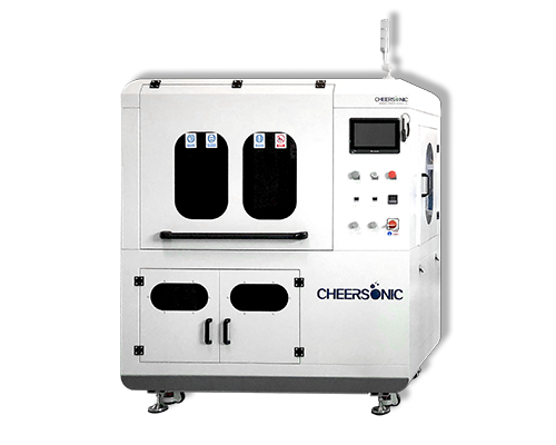
The ultrasonic spraying system can precisely control the flow rate, coating speed and deposition volume. Low-speed spray shaping defines atomized spray as a precise and controllable pattern to avoid excessive spray when producing a very thin and uniform layer. The ultrasonic spray system can control the thickness from sub-micron to more than 100 microns, and can coat any shape or size.