
What is Semiconductor
Before the discovery of semiconductors, people believed that materials in the world could only be divided into “conductive” and “non-conductive (insulating)” according to the classification of conductivity. According to the principle of “mutual independence and complete exhaustion” in the classification method, this is a very perfect classification method for materials in the world. Why does the classification of “semiconductor” still exist?
In some documents, “semiconductor” is defined as “material with conductivity between conductor and insulator”. To be precise, semiconductor material is not in the middle of the two, but its conductivity can be controlled and switched between them. This kind of conductive property can be controlled and switched between conductor and insulator, which is called semiconductor material.
The first discovery of the semiconductor phenomenon dates back to 1833, nearly 200 years ago. Faraday, the father of electronics, found that the resistance of silver sulfide varies with temperature, which is different from that of ordinary metals. Temperature can control the conductivity of silver sulfide materials. This is the first observation of the semiconductor phenomenon.
During the period of more than 100 years from 1833 to 1945, physicists conducted in-depth research on this phenomenon. The physical revolution at the beginning of the 20th century laid a solid theoretical foundation for semiconductor technology, while the material growth technology laid a material foundation for the realization of semiconductor technology.
Ultrasonic spraying technology is used for semiconductor photoresist coating. Compared with traditional coating processes such as spin coating and dip coating, it has the advantages of high uniformity, good encapsulation of microstructures, and controllable coating area. In the past 10 years, it has been fully demonstrated that the 3D microstructure surface photoresist coating using ultrasonic spraying technology, the prepared photoresist coating is significantly higher than the traditional spin coating in terms of microstructure wrapping and uniformity Craft.
The ultrasonic spraying system can precisely control the flow rate, coating speed and deposition volume. Low-speed spray shaping defines atomized spray as a precise and controllable pattern to avoid excessive spray when producing a very thin and uniform layer. The ultrasonic spray system can control the thickness from sub-micron to more than 100 microns, and can coat any shape or size.
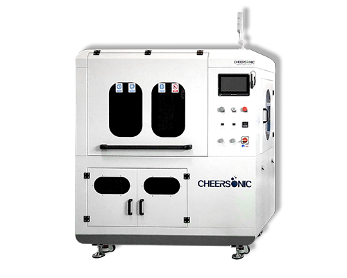
About Cheersonic
Cheersonic is the leading developer and manufacturer of ultrasonic coating systems for applying precise, thin film coatings to protect, strengthen or smooth surfaces on parts and components for the microelectronics/electronics, alternative energy, medical and industrial markets, including specialized glass applications in construction and automotive.
Our coating solutions are environmentally-friendly, efficient and highly reliable, and enable dramatic reductions in overspray, savings in raw material, water and energy usage and provide improved process repeatability, transfer efficiency, high uniformity and reduced emissions.
Chinese Website: Cheersonic Provides Professional Coating Solutions